Hdlbits-Dual-Edge Triggered Flip-Flop
Di: Amelia
Each output bit behaves like a SR flip-flop: The output bit should be set (to 1) the cycle after a 1 to 0 transition occurs. The output bit should be reset (to 0) at the positive clock edge when reset is high. If both of the above events occur at 1. Dflip-flop module top_module( input clk, input d, output reg q); always@(posedge clk)begin q <= d; end endmodule 2. Dflip-flops Create 8 D triggers. All DFF s shall be triggered by the rising edge of clk. module top_module ( input clk, input [7:0] d, output [7:0] q ); always@(posedge clk)begin q <= d; end endmodule 3. DFF with reset Create 8 D flip A dual-edge triggered flip-flop is triggered on both edges of the clock. However, FPGAs don't have dual-edge triggered flip-flops, and always @ (posedge clk or negedge clk) is not accepted as a legal sensitivity list.
3.2.1.18 Dual-edge triggered flip-flop 问题描述:实现双边沿触发的DFF 给的提示:在FPGA中不能通过【always @ (posedge clk or negedge clk)】的写法来生成双边沿触发的DFF,可以通过分别写【always @ (posedge clk)和always @ (negedge clk)】两个块来模拟其行为 提示 By doing so, flip-flop might operate at 1.2Volts, with the novel quick latch and conditional precharging. This paper aims at a new proposed low power dual edge triggered flip-flop with speed enhancement to achieve low power consumption with a shorter delay in power usage, hence, it is well suited for low-power digital system applications. A dual-edge triggered flip-flop is triggered on both edges of the clock. However, FPGAs don’t have dual-edge triggered flip-flops, and always @ (posedge clk or negedge clk) is not accepted as a legal sensitivity list.
VLSI SoC Design: Dual-Edge Triggered Flip Flop

Mux and DFF (Solution: 2014_q4a.v) DFFs and gates (Solution: ece241_2014_q4.v) Create circuit from truth table (Solution: ece241_2013_q7.v) Detect an edge (Solution: edgedetect.v) Detect both edges (Solution: edgedetect2.v) Edge capture register (Solution: edgecapture.v) Dual-edge triggered flip-flop (Solution: dualedge.v) HDLbits刷题Day17(Create circuit from truth table~ Dual-edge triggered flip-flop) 小菜鸡-木子 于 2022-09-13 21:59:40 发布 阅读量365 收藏 2 点赞数 2
HDLBits刷题Day12,3.2.1.17 Edge capture register – 3.2.1.18 Dual-edge triggered flip-flop weixin_52312830 于 2024-02-19 22:12:40 发布 阅读量900 收藏 15 点赞数 16
A dual-edge triggered flip-flop is triggered on both edges of the clock. However, FPGAs don’t have dual-edge triggered flip-flops, and always @ (posedge clk or negedge clk) is not accepted as a legal sensitivity list.
—– 81. D flip-flop —– Problem Statement A D flip-flop is a circuit that stores a bit and is updated periodically, at the (usually) positive edge of a clock signal. D flip-flops are created by the logic synthesizer when a clocked always block is used. A D flip-flop is the simplest form of “blob of combinational logic followed by a flip-flop” where the combinational logic portion is 前言 今天下午更新了一篇博客,对于博客中的一个问题我觉得有必要再深入探讨一下,那就是双沿采样电路。 题目 Build a circuit that functionally behaves like a dual-edge triggered flip-flop: 方法一
在FPGA設計中,雙邊緣觸發器(dual-edge triggered flip-flop)是一種在時鐘信號的上升沿和下降沿都能觸發的觸發器。這種設計可以在每個時鐘週期內進行更多的操作,從而提高系統的效率。然而,FPGA本身並不直接支持雙邊緣觸發器。
In this paper, a technique for implementing low-power Dual Edge Triggered Flip Flop (DETFF) is introduced. Dual edge triggered flip flops has many advantages in low power VLSI compared to SETFF. The Proposed low power DETFF is implemented and compared with conventional DETFF at same simulation conditions. CAD tool based simulation and comparison between the non README.md Tips.md HDLBits_Solution / 3 Circuit / 3.2 Sequential Logic / 3.2.1 Latches and Flip-Flops / 3.2.1.17 Dual-edge triggered FF.v Cannot retrieve latest commit at this time.
What is Dual Edge Triggered Flip Flop? How to design it?
In this question it seems like that a simple delay may work but its not working. I also tried with dual edge triggered flip flops but no luck. Cant figure out the appropriate combinational logic.
Dual-edge triggered flip-flop is a sequential element which samples data at both positive as well as negative edges of the clock. This might come in handy in applications where the throughput is very high. 3.2.1.17 Edge capture register 当监测到输入信号`in`从高电平跳变的低电平时,输出信号`out`会在下一个时钟上升沿输出`in`前一个状态,并一直保持,直到复位信号`reset`有效时(高电平有效),才能将输出信号`out`置为低电平
Detect an edge Detect both edges Edge capture register Dual-edge triggered flip-flop Counters Four-bit binary counter Decade counter Decade counter again Slow decade counter Counter 1-12 Counter 1000 4-digit decimal counter 12-hour clock Shift Registers 4-bit shift register Left/right rotator Left/right arithmetic shift by 1 or 8 5
1.D flip-flop 2.D flip-flops 3.DFF with reset 4.DFF with reset value 5.DFF with asynchronous reset 6.DFF with byte enable 7.D Latch 8.DFF 9.DFF 10.DFF+gate 11.Mux and DFF 12.Mux and DFF 13.DFFs and gates 14.Create circuit from truth table 15.Detect an edge 16.Detect both edges 17.Edge capture register 18.Dual-edge triggered flip-flop
HDLBits中文版,标准参考答案
HDLBits学习笔记(81~88)学习阶段:有问题发[email protected]大家一起讨论。 题目81 Dff题干:D flip-flops are created by the logic synthesizer when a clocked always block is reset to 0 used (See alwaysblock2). A D flip-flop is the simplest form of “blob of combinational logic followed by a flip-_active high asynchronous reset
A D flip-flop is a circuit that stores a bit and is updated periodically, at the (usually) positive edge of a clock signal. D flip-flops are created by the logic synthesizer when a clocked always block is used (See alwaysblock2). A D flip-flop is the simplest form of „blob of combinational logic followed by a flip-flop“ where the combinational logic portion is just a wire. Sequential Logic Latches and Flip -Flops D Flip-Flop A D flip-flop flop is triggered on is a circuit that stores a bit and is updated periodically, at the (usually) positive edge of a clock signal. D flip- flops are created by the logic synthesizer when a clocked always block is used (See alwaysblock2). A D flip-flop is the simplest form of “blob of combinational logic followed by a flip-flop” where the https://hdlbits.01xz.net/wiki/Dualedge 在hdlbits上dual edge flip flop 小弟code 如下 module top_module ( input clk, input d,
Hier sollte eine Beschreibung angezeigt werden, diese Seite lässt dies jedoch nicht zu. 第一题:D flip-flopmodule top_module( input clk, // Clocks are used in sequential circuits input d, output reg q ); always @(posedge clk) begin q <= d; end endmodule第二题:D flip-flopsmodule top
For each bit in an 8-bit vector, detect when the input signal changes from one clock cycle to the next (detect any edge). The output bit should be set the cycle after a 0 to 1 transition occurs.
12 Mux and DFF | 多路复用器和 D 触发器 13 DFFs and gates | D 触发器与门电路的组合 14 Create circuit from truth table | 根据真值表设计电路 15 Detect an edge | 正边沿检测 16 Detect both edges | 双边沿检测 17 Edge capture register | 边沿捕获寄存器 18 Dual-edge triggered fip-fop | 双沿触发 A dual-edge triggered flip-flop is triggered on both edges of the clock. However, FPGAs don’t have dual-edge triggered flip-flops, and always @ (posedge clk or negedge clk) is not accepted as a legal sensitivity list. A dual-edge triggered flip-flop is triggered on both edges of the clock. However, FPGAs don’t have dual-edge triggered flip-flops, and always @ (posedge clk or negedge clk) is not accepted as a legal sensitivity list.
A dual-edge triggered flip-flop is triggered on both edges of the clock. However, FPGAs don’t have dual-edge triggered flip-flops, and always @ (posedge clk or negedge clk) is not accepted as a legal sensitivity list.
-Dual-edge-triggered Flip-Flops
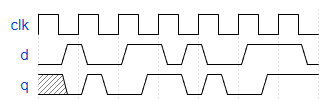
Probelm 97 Dual-edge triggered flip-flop 我们现在对时钟上升沿与下降沿都已经很熟悉了。但是 FPGA 没有一个同时检测双边沿的触发器,而且always中的敏感列表也不支持 (posedge clk or negedge clk)。 牛刀小试 设计一个双边沿检测的触发器,时序如下图所示: Generally, there’s no reason to have a both-edge output reg q always posedge flip-flop inside the FPGA fabric. I realize that you’re doing an exercise, but in most FPGAs it won’t work because of clock routing. That said, It Would Be Nice if the FPGA synthesis tools were smart enough to
这个题博主完全是根据时序图来做的,具体含义博主也不太明白。 更新:博友“ 尔喀索斯 ”给出了解答是 保存32位矢量in下降沿的变化,这个解答是对的,也就是题目要求的不只是下降沿检测,即输出不只是脉冲信号,而是检测到一次下降沿就一直将输出保持为高电平。 3.2.1.18 Dual-edge triggered flip 前言 HDLbits网站如下 Problem sets – HDLBits (01xz.net) 从本期开始我们继续HDLbits第三章Circuits的学习,本期的内容是3.2.1 Latches and Flip-Flops
81. D flip-flop Problem Statement A D flip-flop is a circuit that stores a bit and is updated periodically, at the (usually) positive edge of a clock I’m working on the HDLBits https://hdlbits.01xz.net/wiki/Dualedge But I have a little question about this test, how can I test dual-edge just with the input clk, input d and output q?
- Heimatlexikon Thaleischweiler-Fröschen
- Heimatstube In Quakenbrück | Beliebte Restaurants in Quakenbrück
- Heimat Probierpaket Hof-Pute , Bio Nassfutter für Hunde
- Heilige Schrift Des Islams | Heilige Schrift Koran
- Hazır Mantı Yapılışı , Hazır Mantı Pişirme Tarifi
- Haus Seehund Fewo 15 , Ferienwohnung Seehund, Norderney, Frau Claudia Heise
- Heckboxen, Transportboxen, Stauboxen Für Ahk Träger
- Hedi Schneider Steckt Fest Blu-Ray Online Kaufen
- Hautarzt Rüsselsheim Innenstadt
- Haus Mieten In Klütz _ Immobilien mieten in Boltenhagen, Nordwestmecklenburg